
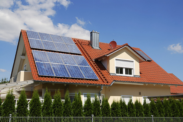
If you’re thinking of installing a residential solar system, there are multiple components to consider, costs to analyze, and decisions to make. Prior to installation, you’ll do a lot of research and you’ll talk to a lot of professionals who will guide you in the steps toward your residential solar system installation. One of the key components, if not THE key component of the system is the solar panel itself.
What are Solar Panels?
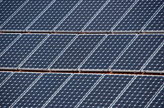
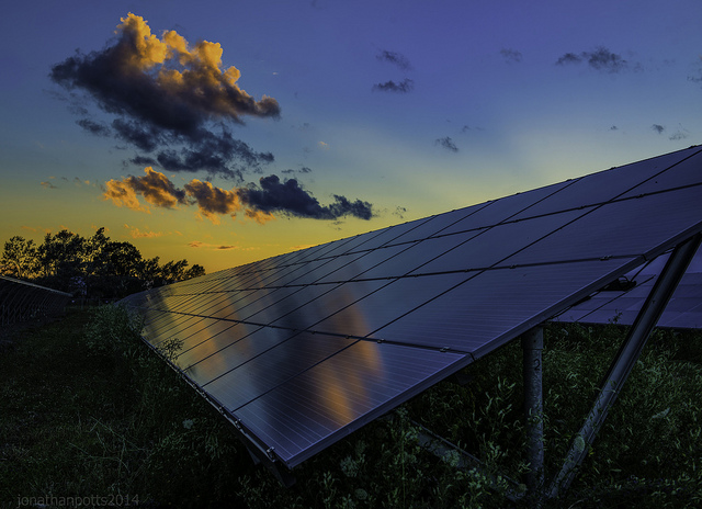
Solar panels consist of solar cells (photovoltaic cells) that convert sunlight to electricity. The more light that hits the solar cells, the more energy is produced. The solar cell converts sunlight into direct current (DC), and an inverter, also part of the solar panel system, then converts the DC current into alternating current (AC) – the power that your household appliances run off of. The energy runs through your electrical panel box, like energy obtained from the grid. Most residential solar home system owners remain connected to the grid for when there is not enough energy converted through the solar panels to power the house (for example, on cloudy days and at night). This way, they can enjoy uninterrupted power and only pay for the amount they use off of the grid.
How efficient are these solar cells at converting sunlight into energy? That depends on a number of things. The first being the type of solar panel you install.
What are Solar Panels Made Of?
The majority of solar panels are made of either crystalline silicon or thin-film solar cells. As far as residential solar systems go, most homeowners use crystalline silicon panels, as you generally need more of the thin-film alternatives to generate enough energy. This means you need a lot of space to install these types of solar panels. In most cases, homeowners don’t own enough land to make this happen.
Solar panels made out of crystalline silicon are smaller, more efficient, and more costly. Monocrystalline silicon solar panels are the most efficient, as the crystals making up these types of panels are the most pure form. Polycrystalline silicon solar panels are at the mid-level of efficiency, and are formed of multiple crystals, crystallites, making their substance a little less pure, and less efficient compared to monocrystalline silicon solar panels. On average, the monocrystalline silicon panels capture about 18-21% of the energy from the sun, where the polycrystalline silicon panels capture about 15% of the sun’s energy.

Thin-film solar panels are the least efficient out of all, but, that doesn’t mean they are not as cost effective. If you have the land for it, choosing this option is often the cheapest, even if you’ll need more solar panels to generate enough energy from the sun to power your home. The efficiency of these types of panels is about 15% on average. But, they’re more robust in higher temperatures and low light conditions, and they’re easier to install.

How Much Power Do Solar Panels Produce?
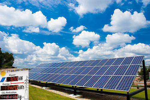
As discussed above, the efficiency of your solar panels is based on a number of things, the type of solar panels you install, your climate conditions, and also the size of the solar system. Solar panels are rated based on the amount of energy they produce, with their output characterized by watts. If you’re shopping for a solar panel system for your home and you see a 300W or 225W system, or your solar engineer recommends a 345W system for your home’s needs, this is referring to the amount of DC current the solar panels will produce, under ideal climate conditions. The average range of residential solar systems is 200 to 350 watts; naturally the higher wattage systems are considered to have superior ratings than the lower output systems. The price you’ll pay for your residential solar panel system will also depend on the wattage. Solar pricing is based on dollar per watt, so the size and wattage of your solar panel system plays a key role in how much your entire solar system will cost you.
Though power is important, it is not the driving factor of how well the solar panels you install will perform. You’ll need to take into account your local climate conditions, the amount of direct sunlight you’ll have once your panels are installed, and also the time of the year. For example, if you live in Seattle, you’ll have considerably less sunlight hitting your residential solar panels, no matter the power or size of your solar panels, compared to someone living in Los Angeles or Arizona – where there is ample sunshine year round. Also, in North America, you’ll have less hours of sunlight during the wintertime, where it can get dark as early as 5pm, compared to the summertime, when the sun doesn’t set until almost 9pm on most nights.
Efficiency of Solar Panels
Now that we’ve discussed what solar panels are, what they’re made of, and how much power they can produce, let’s put all the components together and discuss the efficiency of solar panels.
First things first – what do we mean when we’re talking about efficiency? How well all the components of the system work together? The price for the size of the unit? Not quite. In simplest of terms, solar panel efficiency refers to how much of the sunlight hitting the solar panels successfully gets converted to DC power. If you’re thinking at least half of the sunlight hitting solar panels is able to be used to power your home, your estimates are a little out of reach. At the time of this article, the highest efficiency solar panels capture about 24% of the sun’s energy and convert it into DC power. However, as time marches on, the efficiency will likely increase as well. The actual range of efficiency, dependent of course on the types of panels you have installed, and other climate conditions, can range anywhere from 5% to 24%. Let’s break it down and take a look at what can impact your residential solar panel efficiency rates.
When you’re looking to install a solar energy system for your home, you’re likely going to be talking to multiple solar contractors who will consult with you and provide you their recommendations and estimates for installation. A solar contractor who is trying to sell you a monocrystalline silicon solar panel will likely sell this product based on its high efficiency rating compared to other types of solar panels. But, how much of an effect does this efficiency rating have on the amount of power produced by your system? If you install a 5kwh solar energy system in your home, and opt for higher efficiency solar panels that rate at a 17% efficiency, will you get more power from this system than a 5kwh system with 13% efficiency panels? Nope. Solar panel efficiency is taken into account when rating solar panels. So, if you buy two 250w solar panels, maybe one is monocrystalline silicon and the other is polycrystalline silicon, they’ll both output 250w of power, under ideal temperature and climate conditions.
So, why would you ever buy the most expensive types of solar panels then? Well, you won’t need as many solar panels if they are more efficient in converting sunlight into energy. So, in homes where you do not have a lot of space to install solar panels, these premium panels are likely the better option to get the power production you need.
Another plus for buying more premium solar panels? These types of panels are more often produced by some of the top engineers in the market and might be more on the cutting edge of technology, making their overall quality and reliability an advantage. With the rate of change in the solar energy though, and the rates dropping almost daily, this might not be as strong of a decision factor when considering your options.
In summary, the top factors that will affect the amount of power your system will produce are dependent on the following things:
* The panels’ rated power output
* Solar panel efficiency (based on type of solar panels)
* Temperature sensitivity of your residential solar system
* Degree of shading your panels will see
* The climate you live in (high sun vs. low sun)
* The time of year (winter – shorter days vs. summer – longer days)
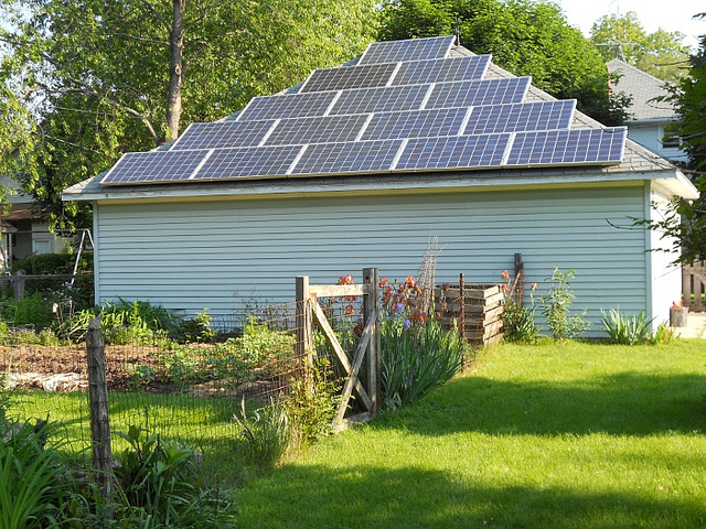
* Angle/type of installation of the solar panels (roof vs. ground)
In Conclusion
Based on what we’ve learned about solar panel efficiency, types of solar panels, size of the system, and the amount of power produced, how do you make your decision? Ultimately, the best route is to choose the residential solar energy system that would produce the most power for what you can afford and for what your home can endure (i.e., will your roof be able to support the weight of the amount and type of solar panels you are looking to install?).
When you choose the a system based on these factors, you’ll maximize your energy output, minimize your energy bills, and see faster returns on investment in the long run.